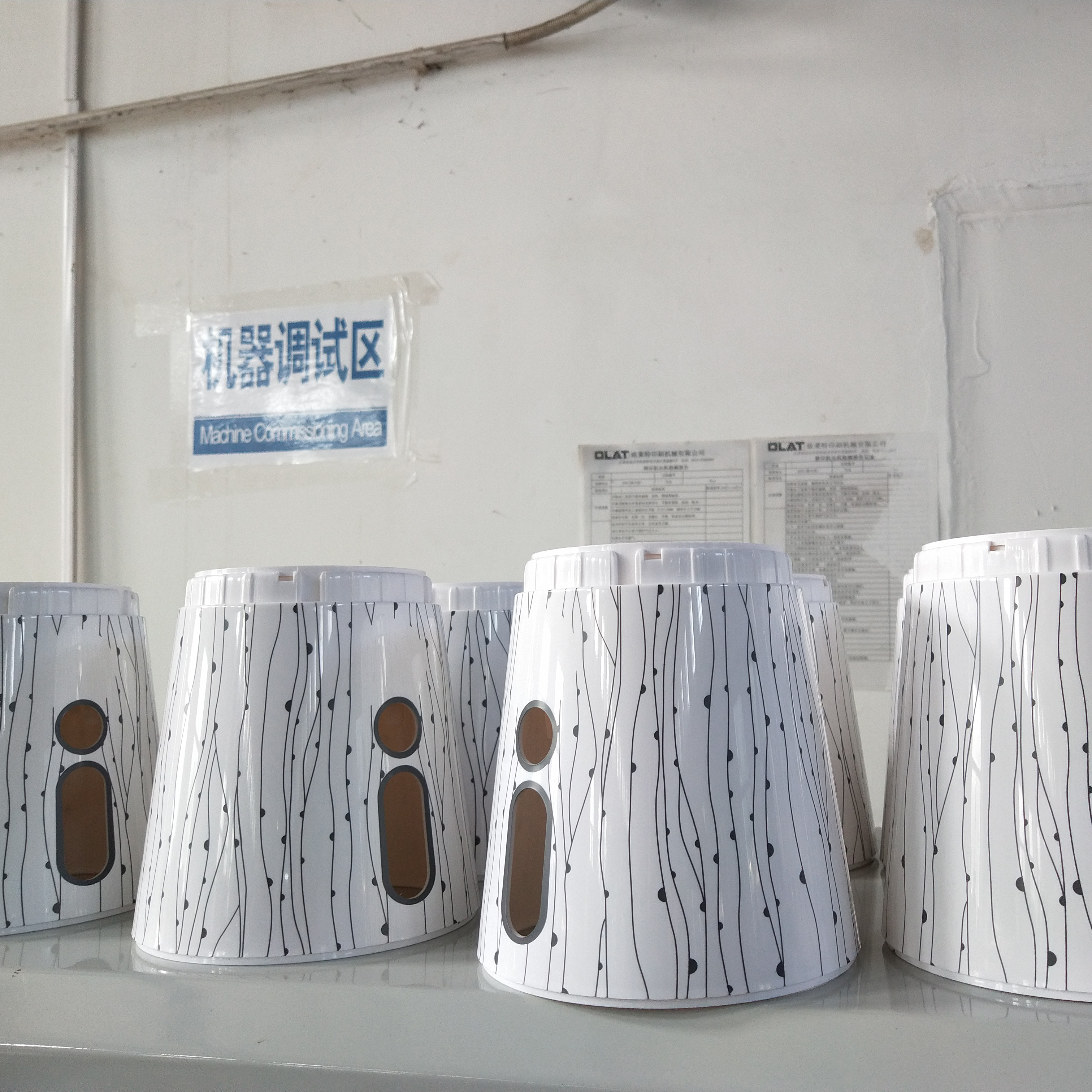
What is a curved screen printing machine? What are the advantages? The circular bottle screen printing machine is a type of screen printing machine, which is specially used to print on various regular curved objects, such as cylindrical bottles, conical table-shaped objects, etc. The following is a detailed introduction about the round bottle screen printing machine: 1. Definition and scope of application. The round bottle screen printing machine prints pictures and texts on round bottles or other curved objects through screen printing. It is suitable for the printing of various cylindrical packaging containers such as cosmetic bottles, medicine bottles, and food bottles, and is also suitable for other objects with regular curved surfaces. 2. Advantages High-precision printing: The round bottle screen printing machine adopts advanced printing technology and equipment, which can achieve high-precision printing, ensuring clear graphics and bright colors. Strong adaptability: This equipment is not only suitable for round bottles, but also for other curved objects of various shapes, such as cone shaped, arc-shaped, etc., with strong adaptability. Efficient production: Round bottle screen printing machines are usually equipped with automated control systems, which can achieve continuous and efficient printing production and improve production efficiency. Cost savings: with
 English
 English